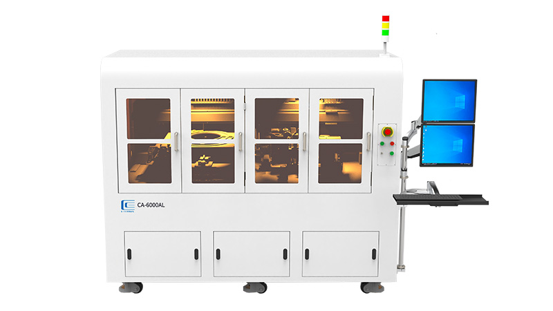
The system is applicable to the pick-and-place, positioning, testing, and sorting of chips after wafer dicing. It adopts a fully automated operation process and can perform high-speed and high-precision chip testing. The average testing time per single chip can be compressed to within seconds, representing a significant improvement in efficiency compared to traditional methods. The system injects new development momentum into the semiconductor packaging and testing industry.
Wide range of applications | |
High accuracy and repeatability | |
High automation | Automatic calibration, real-time fault diagnosis, and predictive maintenance Loading and unloading supports blue tape or chip adsorption box for various forms Automated chip handling system for fast pickup, positioning, testing, and sorting
|
Flexibility | Support OO/OE/EE/RF testing, etc. Fully automated chip testing workflow with intelligent data analysis Parallel testing technology enhances throughput and reduces per-unit cost Supports single/4/8-channel coupled chip testing with high alignment precision
|
All Information given here is reliable to our best knowledge. No responsibility is assumed for possible inaccuracies or omissions. Specifications and external appearances are subject to change without notice.